Pinkerton's video was created to illustrate the real-time flow of security data, transforming overwhelming crime analytics into actionable insights. In the enterprise risk management sector, security professionals struggle to synthesize disparate data points to protect regional assets. Without predictive threat intelligence, organizations face uninformed resource allocation and elevated vulnerability across multi-location operations.
Our design team at Advids established a clean, high-contrast dark visual framework to anchor this security intelligence platform walkthrough. The composition displays a structural US map utilizing regional color overlays, shifting from safe green to high-risk red to instantly categorize threat levels. Circular focus indicators highlight specific state boundaries alongside clear numerical rankings and percentage risk gauges, presenting complex data points in an intuitive hierarchy. We framed these layouts to establish immediate context so that Security Directors instantly grasp the critical safety profiles of their operating territories.
The motion design utilizes targeted map zoom-ins and precise circular scanning indicators to guide the eye directly to critical risk regions. We synchronized these transitions with fluid graphic updates on the risk gauges to structure a cohesive digital platform walk-through. This tactical movement coupled with the clean interface design minimizes cognitive fatigue, allowing viewers to absorb complex geographical rankings without visual clutter. Ultimately, this authoritative visual execution builds deep trust in the underlying data, encouraging Security Directors to confidently integrate these insights into their proactive risk mitigation strategies.
Maximize Prospect Engagement: App Demo Video Production
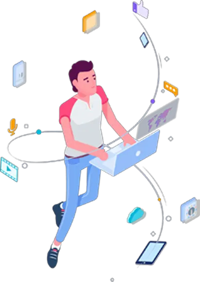
We translate your app's brilliance into clear, engaging visuals. We transform complex technical concepts into accessible visual guides that accelerate lead qualification within your sales funnel.
Hear our Customer's Experience
Real stories from founders and marketing leaders who partnered with Advids to bring complex ideas to life.
6000+ Videos created for 3400+ startups and enterprises
Discuss your video brief to get a video proposal & fixed budget upfront.
Independent B2B Video Production Assessment
4.33/5 (762 Verified Client Audits)
Loved by brands worldwide
"ADVIDS produced several videos over the years for us. They are very responsive and communicative during the entire video production process."
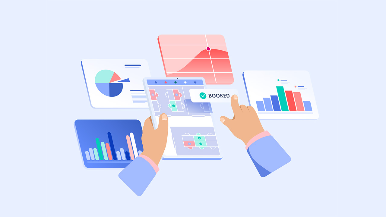
Showcase Functionality
- Effective app demo videos go beyond simple explanations, they provide potential users with a tangible feel of the user experience, driving engagement and downloads.
- Engaging app demo videos simplify complex features, making it easier for your audience to understand and appreciate your app's value proposition.


Checkout Video Work

World Class Video Service
Video Research, Concept, Script & Production. We do it all.
From the first strategic brief to the final polished frame, our in-house specialists handle every stage of your App Demo video so your message resonates with clarity and impact.
Meet Our CreatorsYour App Demo video Partners
Advids is a crew of kind, thoughtful creatives specializing in crafting compelling app demo videos since 2012. We are UI/UX designers, mobile app specialists, scriptwriters, voiceover artists, animators, and video editors dedicated to showcasing your app's brilliance. We've been called app demo video experts, mobile app showcase masters, top-tier app explainer video producers, UI/UX visualization gurus, and more. But above all else, we're your app demo video production partners.
Let's get curious, dive in, and discover how Advids can create an app demo video that elevates your brand and drives downloads. Our team's combined experience in mobile app development and video production ensures a deep understanding of user behavior and effective storytelling, resulting in demos that resonate with your target audience.
App Demo Video Examples From Our Portfolio
ActiveCollab
ActiveCollab's video was engineered to highlight the synchronization of decentralized, global teams working within their project management software. In the collaborative workspace industry, team leads struggle to balance resource capacity management without clear visibility into tracked hours versus estimations. This structural gap often forces organizations to absorb the cost of over-allocated resources, resulting in operational bottlenecks. Our team structured the narrative to show how resolving these coordination challenges prevents project delays.
We anchored the visual layout in actual platform interfaces, presenting a clean workload grid and structured task detail panels that demonstrate practical day-to-day utility. By integrating this resource planning tool preview directly into real-world scenarios, the visual design guides the viewer through the configuration of member permissions and workload allocations. We structured the desktop and mobile interface mockups to highlight clean margins, bold data indicators, and clear toggle buttons. This structured layout emphasizes simplicity over complexity so that Project Managers immediately grasp the business value of restricting edit permissions on critical project timelines.
To bring these features to life, Advids utilized controlled vector transitions and smooth software panning to trace the movement of tasks across the timeline. We framed this application capability summary within a calming, low-contrast pastel palette designed to minimize visual noise and prevent cognitive fatigue for busy coordinators. Gentle zoom-ins highlight specific menu dropdowns and calendar indicators, mimicking a natural user workflow. The resulting demo delivers an authoritative yet approachable tour of the platform, fostering trust and prompting team leaders to modernize their operational workflows.
Citrix
Citrix's video was produced to isolate and spotlight a critical new clinical authentication integration, ensuring immediate user comprehension. In high-pressure medical environments, clinicians lose valuable seconds navigating repetitive logins and manual password entry. This persistent operational lag leads to clinician burnout and administrative friction, while insecure endpoints threaten patient data privacy. Failing to streamline these access points with secure badge-based authentication results in compounded technical debt and decreased patient face-time, costing clinics critical care opportunities.
Our design team anchored this clinical authentication workflow preview in a highly structured dual-pane format. We established a clean split-screen layout that positions a real-world workstation visual adjacent to the active software user interface. On one side, a high-fidelity image displays a proximity card approaching a physical reader, aligned with the digital login sequence on the other. By presenting the distinct user interface panels for Alice and Bob within simulated clinical patient charts, our composition maps the precise login sequence so that Clinicians immediately grasp the functional value of the integration.
We applied rapid, crisp UI transitions that mirror the immediate feedback of the physical hardware integration during this platform interface walkthrough. At Advids, our animation strategy employs clean vertical wipes and instant screen updates to demonstrate high-speed user switching without visual clutter. The structured layout utilizes a unified corporate-blue and neutral palette to reduce cognitive load and prevent clinician fatigue during dense data navigation. This authoritative, step-by-step visual demonstration builds deep operational trust, leading viewers directly to the final technical preview engagement.
Github
GitHub's video was produced to isolate and spotlight a critical new software environment, ensuring immediate user comprehension. In the software development industry, teams frequently face massive productivity drains when transitioning from tracking a bug to actually writing and testing the fix. Without an integrated flow, the cost of inaction is severe: prolonged sprint cycles, rising technical debt, and cognitive fatigue from constant context switching across disconnected tools. At Advids, our team recognized that the visual demonstration needed to bridge this gap.
We anchored the visual architecture of this developer environment visual guide in a highly structured, UI-centric layout that mirrors the natural step-by-step cognitive path of an engineer. We mapped the progress from a static GitHub issue down to an interactive, editable specification panel where current and proposed logic are cleanly segregated. The interface layout highlights file-specific planning nodes and code changes side-by-side with an operational live-preview sandbox. By structuring the screen real estate with clear focal hierarchy and high-contrast division, we ensured that Developers and Engineering Leads immediately grasp how a single click moves an idea directly into a functional codebase.
The motion design relies on smooth, sequential transitions that mimic a real-time logical pipeline, translating abstract code generation into a tangible, linear progression. This functional product walk-through utilizes elegant interface sweeps and precise focal zooms to guide the viewer's eye through complex file trees without inducing visual strain. We balanced the tech-forward, dark-mode aesthetic with clean typography and soft, glow-on-dark focal accents to prevent cognitive fatigue during dense data-flow sequences. The authoritative, rhythm-driven progression builds confidence in the platform's execution, closing with a clear direction that encourages direct workspace adoption.
Venly
Venly's video was created to define the expanding ecosystem of tools living within their unified platform. Operating in the highly technical decentralized application space, the company provides the essential infrastructure required to launch digital assets. Without these integrated developer tools, brands face extreme developer overhead, prolonged time-to-market, and high technical debt. Our team engineered this narrative to show how simplifying blockchain abstraction solves these costly deployment bottlenecks.
We built the static visual architecture of the video on clean, segmented UI cards that isolate and explain complex digital tools. This Web3 developer tool walkthrough highlights critical features like the Venly Wallet UI, which illustrates social sign-in APIs, and the Shopify NFT App interface, which displays branded digital storefronts. By organizing these screens with modular layouts and intuitive hierarchies, our team ensured that Product Managers immediately grasp the platform's simplified integration flow.
The motion design relies on dynamic transitions and logical data-flow animations to track how assets move from the developer console to the user's screen. This functional platform demonstration utilizes a high-contrast, glowing neon palette layered over deep backgrounds to reflect Web3 innovation while ensuring text remains highly readable. Advids engineered these visual pathways to minimize cognitive fatigue, guiding the viewer's attention naturally through each product component. The clear structural rhythm builds immediate trust and establishes the brand as the authoritative choice for enterprise Web3 adoption.
Service Catalogue
How Advids pricing work for App Demo Videos?
Advids offers transparent, value-driven App Demo video pricing with fixed fees for predictable budgeting. We deliver a premium production experience with streamlined workflows, dedicated project management, creative strategy, and complete transparency with no hidden costs.
Take an example of a 60-second App Demo video designed to introduce a product, service, platform, or brand story. The goal: engage audiences, communicate value clearly, and drive stronger customer action.
Clean Design
$1000–1500Simple, polished visuals with clean animation and clear messaging. Ideal for concise storytelling and effective audience engagement.
Engaging Visuals
$1500–2000Enhanced motion graphics, dynamic transitions, and visually engaging scenes designed to increase viewer retention and brand recall.
Strategic Storytelling
$2000–3000Combines compelling narratives, branded visuals, and data-driven messaging to create stronger emotional connection and audience trust.
Advanced Animation
$3000–4500Features advanced animation techniques, premium motion design, and detailed visual sequences for a more immersive viewing experience.
Hybrid Approach
$4500–6000Blends live-action footage, cinematic visuals, animation, and motion graphics to deliver a highly engaging and impactful final production.
What content team from Advids is assigned and their expertise?
At Advids, we dedicate a team of App Demo video specialists to illuminate your brand's message, blending creative storytelling with strategic marketing objectives to deliver App Demo videos that drive results.
Creative Director
Leads the project vision from initial concept and scriptwriting to final production, championing your brand's message through compelling storytelling and innovative visual communication.
Storyboard Artist
Visualizes the narrative flow, sketching key scenes and actions to create a dynamic blueprint, ensuring clarity and engagement for a captivating viewer experience.
Animator
Brings the storyboard to life using cutting-edge animation techniques to create visually stunning, engaging motion graphics and character animation.
Voiceover Artist
Provides the perfect voice to complement your message, conveying information clearly and engagingly while adding personality and emotion to connect with your audience.
Sound Designer
Creates a rich audio landscape that enhances emotional impact, expertly blending music, sound effects, and voiceover into an immersive auditory experience.
Video Editor
Polishes the final product, seamlessly integrating animation, voiceover, and sound design to ensure a smooth, professional result that maximizes visual appeal and engagement.
What experience Advids has in App Demo Video production?
Advids expertly crafts compelling app demo videos showcasing functionality and user experience through concise narratives and visuals. We offer diverse 3D walkthrough styles: interactive demos, Feature Highlights , immersive explorations, and Gamified Tutorials . Our videos leverage mobile App Design and User Behavior research to boost downloads and engagement. We excel at conceptualizing, designing, and creating 3D walkthrough videos aligned with your app's Value Proposition and target audience. Our team meticulously crafts seamless and captivating videos.
Across diverse industries (gaming, SaaS, education, healthcare, e-commerce), we transform complex app functions into engaging videos, tailoring each to resonate with specific market expectations and trends. 12 years of experience crafting effective videos has honed our expertise in app demos, explainers, and promotional materials that drive results, reflecting our understanding of evolving App Marketing .
We begin each project with thorough research, analyzing your target audience, competition, and app features. Our innovative storytelling and meticulous planning—from Camera Angle s to animations—create visually stunning videos that drive results (downloads, engagement, in-app purchases). Our 3D walkthrough videos offer immersive explorations of your app's features. We create engaging mobile app explainer videos that clearly communicate your app's value. Our software demo videos showcase functionality and user experience.
Struggling to get your message across?
An App Demo video can be the key. At Advids, we understand the power of clear communication and engaging visuals. We don't just create videos; we craft experiences that resonate with your audience and drive results.
- Imagine a story that captivates your viewers from start to finish — that's what we deliver.
- Our App Demo video Production process ensures your message is clear, concise, and memorable.
- With Advids, you get a partner who is passionate about helping you achieve your goals through effective video.
Production Process
Ready to create an amazing App Demo video? Before diving into script creation, we focus on pre-production — the crucial foundation for success. This detailed pre-production is crucial for your video content marketing strategy.
First, understand your audience, their needs, and what resonates with them.
Next, define clear objectives — what should your App Demo video achieve.
Then, identify your core message — what's the key takeaway you want to convey.
Our App Demo video Production process begins with a deep dive into your needs. As your App Demo video Production agency, we're here to guide you through every step. Effective product video production starts with a solid pre-production plan.