


Elevenlabs
ElevenLabs's video was built to visually prove the immediate financial and temporal ROI of their automation software. In the hyper-growth generative AI sector, managing global user tiers and processing payouts to creators can overwhelm early-stage development teams. Without automated subscription billing systems, companies face compounding technical debt, delayed market entry, and immense operational bottlenecks that stall enterprise-grade scaling. By integrating a centralized billing and payout solution, organizations eliminate the need to build billing engines from scratch, allowing engineering resources to stay focused on core product innovation.
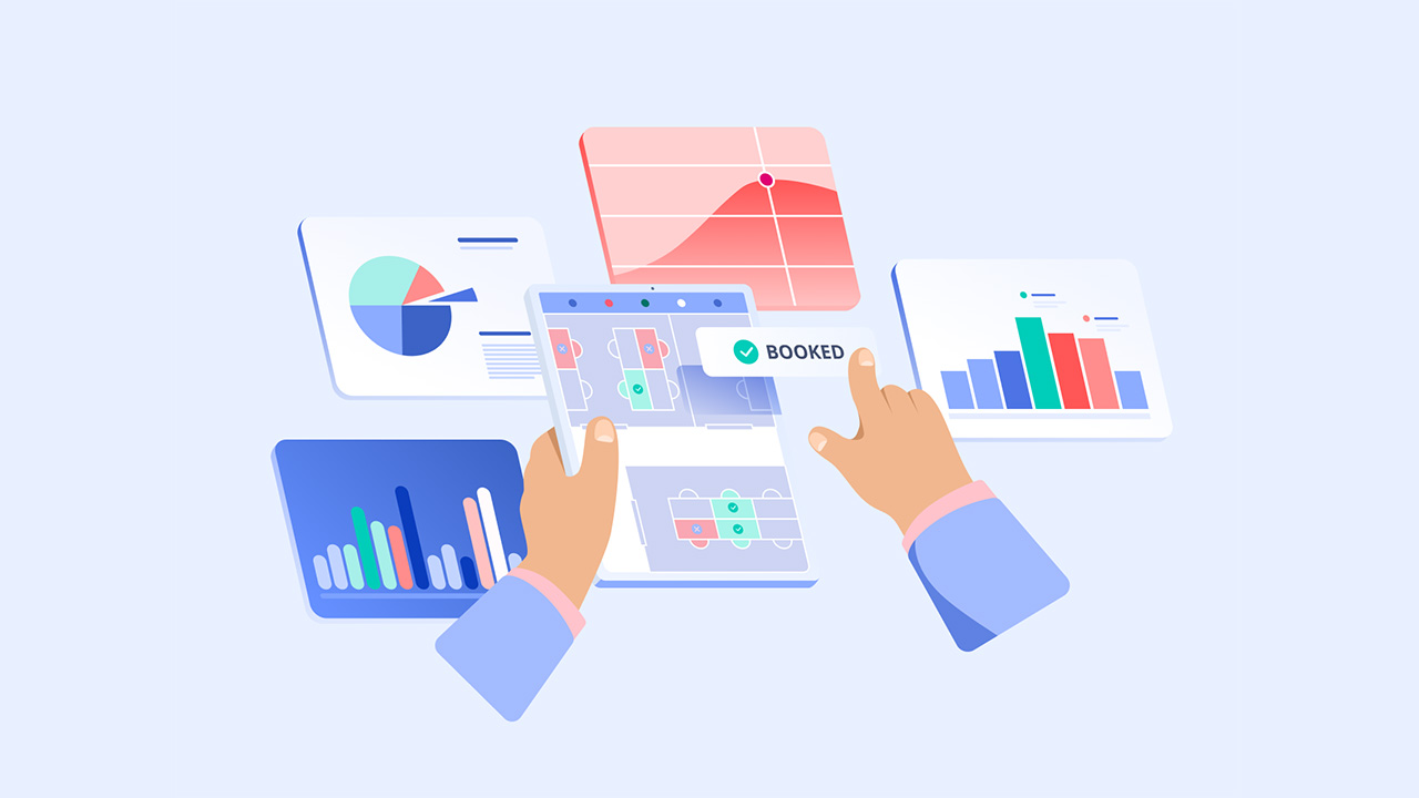
Our design team at Advids structured the user interface overlays to directly complement the high-contrast cinematic studio lighting, presenting complex API endpoints as highly legible, floating UI components. We designed this monetization workflow showcase to display real-time pricing plans, user databases, and developer code repositories side-by-side with clear, color-coded status badges. By mapping out clear visual hierarchies-ranging from multi-tiered subscription pricing structures to automated payout status tracks-we ensured that the visual cues directly support the spoken case study. This visual methodology distills highly technical code deployments into structured, readable steps so that Growth Leads and Tech Founders immediately grasp the business value of ElevenLabs's billing infrastructure.
Our motion design focused on the clean, rhythmic pacing of UI transitions and precise code rendering to maintain high engagement throughout the case study. We timed every interface transition and payout chart update to match the narrative beats, delivering a cohesive platform capability overview that prevents cognitive fatigue. The balanced composition and deliberate pacing of these UI screen walkthroughs drastically reduce information overload for busy stakeholders. By maintaining a professional, authoritative tone, we built deep credibility that effortlessly drives C-Suite Executives toward trusting automated payment integrations.